Difference between revisions of "Minutes-2-23-2012"
From GlueXWiki
(→Agenda) |
|||
| Line 8: | Line 8: | ||
# First package tests [https://halldweb1.jlab.org/elog-halld/FDC/ FDC ELOG] (Beni, Lubomir) | # First package tests [https://halldweb1.jlab.org/elog-halld/FDC/ FDC ELOG] (Beni, Lubomir) | ||
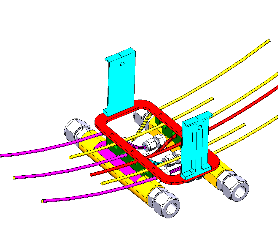
# Engineering update[http://www.jlab.org/Hall-D/detector/fdc/drawings/NEW_MANIFOLD_ASSY2.png],[http://www.jlab.org/Hall-D/detector/fdc/drawings/NEW_MANIFOLD_ASSY1.png cooling manifold] (Bill) | # Engineering update[http://www.jlab.org/Hall-D/detector/fdc/drawings/NEW_MANIFOLD_ASSY2.png],[http://www.jlab.org/Hall-D/detector/fdc/drawings/NEW_MANIFOLD_ASSY1.png cooling manifold] (Bill) | ||
| − | # Electronics update ( | + | # Electronics update (Nick) |
# Other | # Other | ||
| Line 15: | Line 15: | ||
= Minutes = | = Minutes = | ||
| − | Participants: Bill, Dave, | + | Participants: Bill, Dave, Nick, Elton, Mark, Simon, Beni, and Lubomir. |
== Production == | == Production == | ||
| − | - Dave: | + | - Dave: Deadened the first wire plane of package 3 with the larger diameter using the procedure with increased current and the same time as for the smaller diameter, but adding extra polishing cycle. Working on four cathodes now and on the last wire frame for the third package. One more cathode to finish the package. We estimated that for the |
| − | + | ||
- Two more electroplating samples were made. One with the original procedure with extra polishing; before using the same procedure all the wires were fine except one. Second sample with increasing the time instead of the current compared to the 6cm-diameter original procedure, and in addition the polishing current was increased to have a ratio of 3 w.r.t electroplating current. Will be waiting for the microscope pictures from Olga to make a decision. | - Two more electroplating samples were made. One with the original procedure with extra polishing; before using the same procedure all the wires were fine except one. Second sample with increasing the time instead of the current compared to the 6cm-diameter original procedure, and in addition the polishing current was increased to have a ratio of 3 w.r.t electroplating current. Will be waiting for the microscope pictures from Olga to make a decision. | ||
Revision as of 19:27, 23 February 2012
February 23, 2012 FDC meeting
Agenda
- Production Construction Tracking (Dave)
- Production status
- Testing at Blue Crab (Lubomir)
- First package tests FDC ELOG (Beni, Lubomir)
- Engineering update[1],cooling manifold (Bill)
- Electronics update (Nick)
- Other
![[1]](http://www.jlab.org/Hall-D/detector/fdc/drawings/NEW_MANIFOLD_ASSY2.png)