Difference between revisions of "Tagger Microscope"
Senderovich (Talk | contribs) |
Senderovich (Talk | contribs) |
||
| Line 10: | Line 10: | ||
To avoid placing photo-sensors along the path of the electronics, the scintillation light will be delivered to separately-mounted sensors and electronics via clear fiber waveguides. | To avoid placing photo-sensors along the path of the electronics, the scintillation light will be delivered to separately-mounted sensors and electronics via clear fiber waveguides. | ||
| + | |||
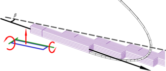
| + | [[Image:ScintPlane_DOFs.png|thumb|335px|Alignment of the scintillating fibers with respect to the electron trajectories. The mounting rails for the scintillators has been designed with degrees of freedom necessary for online-alignment to the electron plane as well as selection of the active fiber row/]] | ||
[[Image:ElectronicsAssy_rend.jpg|thumb|250px|Rendering of the silicon photomultiplier-based scintillating fiber readout electronics.]] | [[Image:ElectronicsAssy_rend.jpg|thumb|250px|Rendering of the silicon photomultiplier-based scintillating fiber readout electronics.]] | ||
Revision as of 20:42, 7 November 2009
Main page: Tagger Microscope Contruction (UConn Wiki)
The Tagger Microscope is a movable, high-resolution hodoscope that counts post- bremsstrahlung electrons corresponding to the photon energy band of interest to the experiment in Hall D. While designed as a general-use device, it has been optimized primarily for use in the GlueX experiment, covering the Eγ range of 8.4-9 GeV (Ee 3-3.6 GeV)
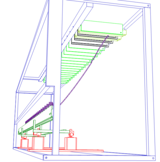
The design of the Tagger Microscope calls for the spectrally-analyzed electron focal plane to be instrumented with a detector array of scintillating fibers with axes oriented toward the oncoming electrons. This is done to maintain fine focal plane segmentation in two dimensions:
- fine segmentation along the direction of electrons spread mitigates the rate and increases the energy resolution
- segmentation in the y-directions allows selective readout to match the photon collimator acceptance.
To avoid placing photo-sensors along the path of the electronics, the scintillation light will be delivered to separately-mounted sensors and electronics via clear fiber waveguides.


